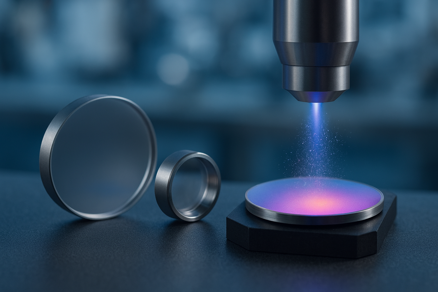
For ultra-precision optical lenses, surface coating is the final and most critical step — the finishing touch that elevates a processed substrate to meet the demanding requirements of its final system. Precision optical coating is far more than simply “adding a thin film.” It requires atomic-scale control over film thickness, material, and structure in order to achieve specific optical properties, such as ultra-high transmission, ultra-high reflection, precise beam-splitting ratios, and extreme environmental stability.
The challenges in optical coating are significant. No supplier can honestly say: “Anything you imagine, I can make happen.” More often, there is a conflict between “what customers want” and “what the process allows.” This is why evaluations are performed with extreme caution. The pursuit of perfection is the very essence of ultra-precision optics, driving the field to constantly push its limits. Today, precision coating technologies are flourishing, with multiple mainstream methods competing and complementing one another. Let’s take a closer look at them.
1. Physical Vapor Deposition (PVD)
This is currently the most widely used technique for precision optical coatings, with two major variants:
(1) Electron-Beam Evaporation (E-beam Evaporation)
Principle:
In a high-vacuum chamber, a high-energy electron beam bombards the coating material (such as SiO₂, Ta₂O₅, HfO₂) placed in a water-cooled crucible. The material melts, vaporizes, and its atoms travel in straight lines to deposit on a rotating substrate surface, forming a thin film.
Characteristics:
-
Advantages: Capable of evaporating high-melting-point materials; relatively fast deposition rate; high purity (avoids contamination from resistive heating sources).
-
Disadvantages: Film structures are typically columnar and porous, leading to water vapor absorption and optical property drift in air, resulting in poor environmental stability.
(2) Ion-Assisted Deposition (IAD)
Principle:
A revolutionary upgrade to E-beam evaporation, IAD has become the standard for modern precision coatings. While the coating material is evaporated, an independent ion source (e.g., a Kaufman source) generates a high-energy inert ion beam (often argon ions) that bombards the growing film.
Key Functions of Ion Bombardment:
-
Increases film density by breaking columnar structures and forming amorphous, bulk-like layers.
-
Reduces internal stress by adjusting ion energy and flux.
-
Enhances adhesion by cleaning and activating the substrate surface.
-
Stabilizes optical properties since dense films absorb little water vapor.
Application:
IAD dramatically improves film mechanical strength and environmental stability, making it the preferred method for high-performance laser optics, astronomical filters, and other demanding applications.
2. Ion Beam Sputtering (IBS)
Principle:
Widely recognized as the highest-precision coating technique. An ion source generates a high-energy beam (typically argon ions) that bombards a target (the coating material), ejecting atoms through physical sputtering. These high-energy atoms then deposit onto the substrate. An auxiliary ion source may also bombard the substrate directly, similar to IAD.
Characteristics:
-
Unmatched Precision: Ultra-slow and stable deposition allows atomic-scale thickness control and extremely sharp interfaces.
-
Extreme Density: Sputtered atoms produce exceptionally dense films with negligible scattering.
-
Ultra-Low Loss: IBS films can achieve reflectivities above 99.999% with minimal absorption, as demonstrated in applications such as LIGO gravitational wave detectors.
Drawbacks: Equipment is expensive, deposition rates are slow, and costs are high.
Applications: High-end fields such as EUV lithography, gravitational wave detection, quantum optics, and space optics requiring exceptional stability.
3. Atomic Layer Deposition (ALD)
Principle:
A film growth method based on self-limiting surface chemical reactions. Precursor gases A and B are alternately pulsed into the chamber. Each pulse reacts with the surface to form a single atomic layer, followed by an inert gas purge to remove excess reactants. Each full cycle deposits one monolayer of compound film.
Characteristics:
-
Perfect Conformality: Coats even deep trenches and complex surfaces uniformly, beyond PVD’s capability.
-
Atomic-Level Control: Thickness is determined by cycle count, accurate to a single atomic layer.
-
High Film Quality: Pin-hole free and highly dense.
Drawbacks: Very slow deposition; limited precursor choices; usually restricted to very thin or functional films.
Applications: Functional coatings in nano-optics, photonic crystals, and protective over-layers for existing optical films.
Key Enabling Factors for Ultra-Precision Coating
Regardless of the technique used, achieving ultra-precision coatings depends on the following critical factors:
-
Accurate Thickness Control Systems
-
Optical Monitoring: Uses a monochromatic laser to track transmission/reflection of a witness sample in real time. Extremely precise but operator-dependent.
-
Quartz Crystal Monitoring: Measures deposition mass via oscillation frequency shifts. Simpler and scalable for production but requires careful calibration.
-
-
Ultra-High Vacuum Environment
-
Chambers typically reach 10⁻⁵ Pa (10⁻⁷ mbar) to ensure long mean free paths for vapor atoms, preventing collisions and contamination.
-
-
Advanced Plasma/Ion Sources
-
The “soul” of modern coating systems, controlling ion energy and flux to determine film density and stress.
-
-
High-Purity Materials
-
Target and evaporation materials must exceed 99.99% purity to avoid defects that reduce laser damage thresholds.
-
| Technology | Principle | Advantages | Disadvantages | Typical Applications |
|---|---|---|---|---|
| E-beam Evaporation | Electron beam heats material for evaporation and deposition | Fast rate, can deposit high melting point materials | Porous film, poor stability | General optical components, decorative coatings |
| Ion Assisted Deposition (IAD) | E-beam evaporation + ion bombardment | Dense film, good stability, cost-effective | Less precise than IBS | High-performance laser mirrors, astronomical filters, automotive/industrial optics |
| Ion Beam Sputtering (IBS) | Ion beam sputters target material to deposit | Highest precision, densest films, lowest loss | Expensive equipment, slow rate | Cutting-edge fields: EUV lithography, gravitational wave detection, quantum computing |
| Atomic Layer Deposition (ALD) | Surface self-limiting chemical reactions | Exceptional uniformity, precise thickness control, excellent durability | Slow rate, limited materials | Nanostructure coatings, protective layers, semiconductor industry |
Summary
Choosing the right coating technology for ultra-precision optics is never straightforward. Each method has distinct strengths and limitations, and the decision often balances performance, cost, and production cycle.
-
IBS represents the current pinnacle of coating precision.
-
IAD is the most mainstream and balanced choice for high-performance applications.
Ultimately, the shared goal of these technologies is to construct perfect artificial structures at the atomic level, enabling light to propagate exactly as humans intend.
This concludes today’s discussion in the series “How Ultra-Precision Optical Lenses Are Made.” In the next chapter, we will explore other fascinating aspects of ultra-precision optics. My mission as a dedicated optics enthusiast is to help you understand the deepest technical principles in the simplest possible language.
Share:
Common Optical Components in the Laboratory
Precision Manufacturing for Advanced Laser Components - Your Partner from Prototype to Production